Simulation of micro and nanoelectronics devices
Electrical
Simulation
of
materials
and
semiconductor
devices
in
2D
and
3D.
Extraction
of
their
operating
characteristics
such
as
current-voltage
(I-V),
capacitance
(C-V,
C-f),
reliability, hot carriers.
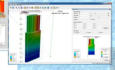
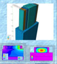
Instrumentation
•
TCAD
simulation
software
for
2D
and
3D
micro
and
nano
devices
(Silvaco
suite:
Devedit,
Athena,
Atlas,
and
Synopsys:
Sentaurus),
with
compatibility
of
simulated
devices to SPICE software.
•
High
performance
computational
system
(computer
network
and
software
in
Linux
and MS Windows) for TCAD calculations.
Publications
1
.
T.A.
Oproglidis,
et.
al.,
Analytical
Drain
Current
Compact
Model
in
the
Depletion
Operation
Region
of
Short-Channel
Triple-Gate
Junctionless
Transistors
,
IEEE
Transactions on Electron Devices 64, 66 (2017).
2
.
D.H.
Tassis,
et.
al.,
Source/drain
optimization
of
underlapped
lightly
doped
nanoscale double-gate MOSFETs
, Microelectronic Engineering 87, 2353 (2010).
3
.
N.
Fasarakis,
et.
al.,
Compact
Capacitance
Model
of
Undoped
or
Lightly
Doped
Ultra-Scaled
Triple-Gate
FinFETs
,
IEEE
Transactions
on
Electron
Devices
59,
3306
(2012).
4
.
C.A.Dimitriadis
and
D.H.Tassis,
On
the
threshold
voltage
and
channel
conductance
of polycrystalline silicon thin-film transistors
J. Appl. Phys. 79, 4431 (1996).
5
.
D.H.
Tassis,
et.
al.,
Low
frequency
noise
in
β-FeSi2/n-Si
heterojunctions
,
Appl.
Phys.
Lett. 72, 713, (1998).


SITE MAP
Home | Personnel | Research |
Services | Projects | Collaborations
| Teaching | Announcements


PHYSICOCHEMICAL
CHARACTERIZATION,
STUDY OF MATERIALS
AND DEVICES